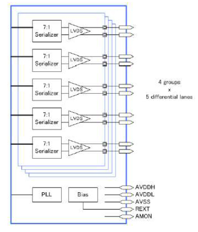
A physical layer IP for LVDS transmitter. This IP consists of 20-lane (4 x 4D1C) LVDS drivers and supports up to 1.5Gbps data rate. In LVDS mode, both the serial and parallel data are organized into 4 channels. The parallel data is 7 bits wide per channel. The input clock is 25MHz to 150MHz. The serializer is highly integrated and requires no external components. The circuit is designed in a modular fashion and desensitized to process variations. This facilitates process migration, and results in a robust design.

LVDS compliant Tx
4 groups of 4-Data
1-Clock channels Each lane/group can be turned on/off individually Data/Clock can be assigned to any lane within the group
Differential polarity can be flip per lane
Supports from 168Mbps to 1.5Gbps data rate
Supports reduced swing mode
X7 Multiplier PLL for serial clock generation
Configurable analog characteristics
PLL loop filter
PLL VCO gain
Differential voltage Common-mode voltage
Pre-emphasis strength
Silicon Proven in GF 28nm SLP
Deliverables
Datasheet
Integration guideline
GDSII or Phantom
GDSII Layer map table
CDL netlist for LVS
LEF Verilog behaviour model
Liberty timing model DRC/LVS/ERC results