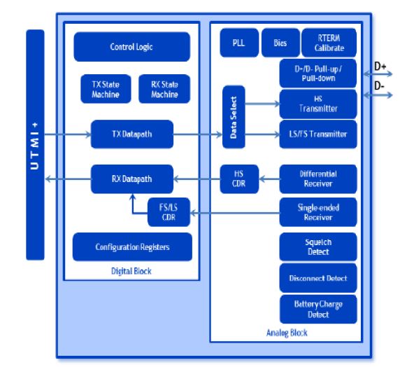
A full physical layer (PHY) IP solution designed for outstanding performance and minimal power consumption is the USB2.0 PHY IP. The USB2.0 IP implements the High-Speed USB 2.0 transceiver, which can be used with hosts, devices, or OTG function controllers. The USB2.0 PHY IP, which supports both Full-Speed (12 Mbps) and Low-Speed (1.5 Mbps) data rates, comes after the UTMI+ level 3 specification. 480Mbps of high-speed data can be transferred by combining numerous mixed-signal circuits. The enhanced USB Battery Charging standards, which are designed for mobile and consumer product applications, are also supported by the USB2.0 PHY IP. Small chip size and low power consumption of the USB2.0 PHY IP transceiver did not compromise performance or data throughput. The USB2.0 PHY IP contains a full on-chip physical transceiver solution with Electrostatic Discharge (ESD) protection, a clock generating block provided by an internal PLL, and a resistor termination calibration circuit in order to fully enable host and device functionality.

Deliverables
Circuit Layout Data with Layer Mapping Information in GDSII
.LEF Files depicting Placement and Routing Aspects
Library of Timing and Power Models in .lib Format
Verilog HDL Description of Circuit Behavior
Circuit Netlist annotated with SDF Timing Constraints
Design Guidelines and Best Practices for Layout Design
Reports confirming Layout Consistency and Design Rule Compliance