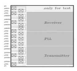
A high performance, high-speed SERDES IP known as USB3.1Type-C PHY was created for Semiconductor IP Cores that allow high bandwidth data transfers while using less power. A specific design for USB 3.1 type-C applications is the USB 3.1Type-C PHY IP. A separate PCS can be provided in addition to the USB 3.1 Type C PHY IP to complete the functionality of various applications, including elastic buffer, scramble/de-scramble, data encoding/decoding, PRBS generation/checking, registers control, and testing. Depending on the customer's request, PCS is offered as either a hard macro or a soft macro. The PCS standard will also be made accessible independently. A test bench created in Verilog HDL is used to validate PHY functionality by the NC-Verilog simulation program.

Deliverables
Graphic Data System II File with Layer Configuration .
LEF Files Containing Placement and Routing Views
Standard Cell Library with Timing and Power Models
Verilog Representation of Functional Behavior
Netlist Annotated with Standard Delay Format Timing Constraints
Application Notes Offering Layout Guidelines
LVS and DRC Verification Results Documentation