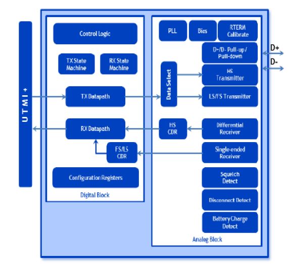
The USB2.0 PHY IP is a comprehensive physical layer (PHY) IP solution created for exceptional performance and low power consumption. The High-Speed USB 2.0 transceiver, which can be used with hosts, devices, or OTG function controllers, is implemented by the USB2.0 IP. The UTMI+ level 3 specification is followed by the USB2.0 PHY IP, which supports both Full-Speed (12 Mbps) and Low-Speed (1.5 Mbps) data rates. Combining numerous mixed-signal circuits can provide high-speed data transmission at 480Mbps. The USB2.0 PHY IP also supports the expanded USB Battery Charging standards, which are intended for mobile and consumer product applications. The USB2.0 PHY IP transceiver's small chip size and low power consumption had no impact on performance or data throughput. In order to fully allow host and device functionality, the USB2.0 PHY IP delivers a full on-chip physical transceiver solution with Electrostatic Discharge (ESD) protection, a clock generating block provided by an internal PLL, and a resistor termination calibration circuit.

Deliverables
GDSII Format with Detailed Layer Mapping
.LEF Views illustrating Placement and Routing Structures
Standard Cell Library featuring Timing and Power Information
Behavioral Model expressed in Verilog Syntax
Netlist Including Timing Annotations in SDF Format
Recommendations for Effective Layout Design and Execution
Validation Reports Ensuring Layout Adherence to Schematic and Rules