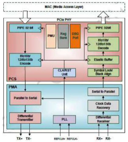
For the high-bandwidth applications, PCIe 3.0 PHY IP offers high-performance, multi-lane capabilities, and low-power design. The PCIe 3.0 IP complies with the PIPE 4.3 standard and supports the whole spectrum of PCIe 3.0 Base applications. High-speed mixed signal circuits are included into the IP to handle PCIe 3.0 traffic at 8Gbps. Both the 2.5Gbps PCIe 1.0 data rate and the 5.0Gbps PCIe 2.0 data rate are backward compatible with it. The needs for various channel conditions may be met by the PCIe 3.0 IP thanks to its support for both TX and RX equalisation approaches.

Compliant with PCIe 3.0 Base Specification
Compliant with PIPE 4.3
Supported data transfer rate: 2.5 GT/s, 5.0 GT/s and 8.0 GT/s
Supported physical lane width: x4
Supported parallel interface: 32-bit
Supported input reference clock: 100 MHz
Supported parallel interface data clock: 62.5 MHz, 125 MHz, and 250 MHz
Supporting low power operation with configurable setting in power state P1/P2/L1 PM Substates:PLL control, reference clock control, and embedded power gating control
Silicon Proven in TSMC 16FFC
Operating Voltage: 0.9V, 0.95V, 1.2V and 1.8V
Providing robust testability by low-cost Build-In Self-Test (BIST) via near-end analog and external loopback interface as well as far-end analog/digital loopback interface
Deliverables
GDSII & layer map
Place-Route views (.LEF)
Liberty library (.lib)
Verilog behaviour model
Netlist & SDF timing
Layout guidelines, application notes
LVS/DRC verification reports