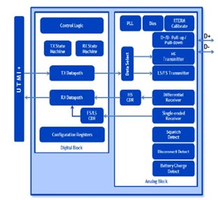
A complete physical layer (PHY) IP solution designed for outstanding performance and minimal power consumption is the USB2.0 PHY IP. The USB2.0 IP implements the High-Speed USB 2.0 transceiver, which can be used with hosts, devices, or OTG function controllers. The USB2.0 PHY IP, which supports both Full-Speed (12 Mbps) and Low-Speed (1.5 Mbps) data rates, comes after the UTMI+ level 3 specification. Several mixed-signal circuits combined can deliver 480Mbps of high-speed data transfer. The enhanced USB Battery Charging standards, which are designed for mobile and consumer product applications, are also supported by the USB2.0 PHY IP. The multiple production facilities and nodes that are present in the USB 2.0 PHY IP include TSMC 28HPC+, TSMC 40LP, TSMC 40LL, UMC 28HPC, UMC 40LP, UMC 55SP, UMC 55EF, SMIC 14SF+, SMIC 40LL, and SMIC 55LL. Performance and data throughput were unaffected by the tiny chip size and low power consumption of the USB2.0 PHY IP transceiver. The USB2.0 PHY IP offers a complete on-chip physical transceiver solution with Electrostatic Discharge (ESD) protection, a clock generating block provided by an internal PLL, and a resistor termination calibration circuit in order to completely enable host and device functionality.

Deliverables
Graphic Data System II File with Layer Definitions
Layout Exchange Format Providing Placement and Routing Views
.lib File Containing Timing, Power, and Noise Characteristics
Verilog Model Describing Functional Circuit Operations
Standard Delay Format (SDF) Timing Applied to Circuit Netlist
Application Notes Offering Insights into Layout Optimization
LVS and DRC Verification Results Documentation