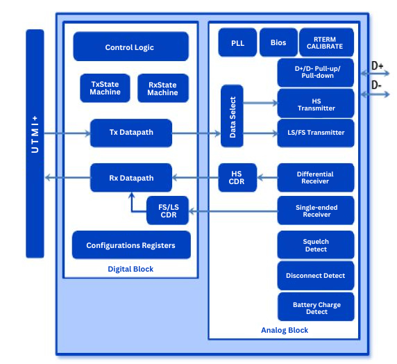
The USB 2.0 PHY IP Core offers a complete physical layer (PHY) solution for high performance and low power. It implements a High-Speed USB 2.0 transceiver compatible with host, device, and On-The-Go (OTG) controllers. Supporting UTMI+ level 3, the PHY also offers backward compatibility with Full-Speed (12 Mbps) and Low-Speed (1.5 Mbps) data rates.
Combined with mixed-signal circuits, it delivers 480 Mbps of high-speed data transfer. Additionally, the USB 2.0 PHY IP supports USB Battery Charging specifications, targeting mobile and consumer products. The transceiver prioritizes low power consumption and minimal die area while maintaining performance and data throughput.
For comprehensive host and device support, it integrates a full on-chip solution with ESD protection, an internal PLL clock generation block, and a resistor termination calibration circuit.
calibration circuit.
Deliverables
GDSII Format with Detailed Layer Allocation
Views of Placement and Routing in .LEF Format
Standard Cell Library with Extensive Timing and Power Characterization
Behavioral Model Expressed in Verilog Language
Netlist Including Timing Annotations in SDF
Recommendations for Effective Layout Design and Execution
Validation Reports Ensuring Layout Adherence to Schematic and Rules