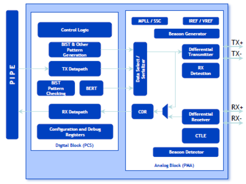
The PCIe 2.0 PHY IP presents a configurable physical layer (PHY) IP solution tailored for Consumer Electronics. It combines mixed signal circuits to facilitate data transfer speeds of both 2.5GT/s and 5.0GT/s, adhering to PCIe 2.0 basic standards. Comprising two layers, namely the Physical Media Attachment (PMA) layer and the Physical Coding Sublayer (PCS), it seamlessly interfaces with the PCIe 2.0 MAC layer through the standard PIPE-3.0 interface.
Designed for minimal power consumption and compact device footprint, the PCIe 2.0 PHY IP transceiver maintains excellent performance and data throughput. It incorporates an on-chip physical transceiver solution featuring ESD protection, an integrated self-test module with built-in jitter injection, and a dynamic equalization circuit ensuring comprehensive support for high-performance architectures.
Deliverables
