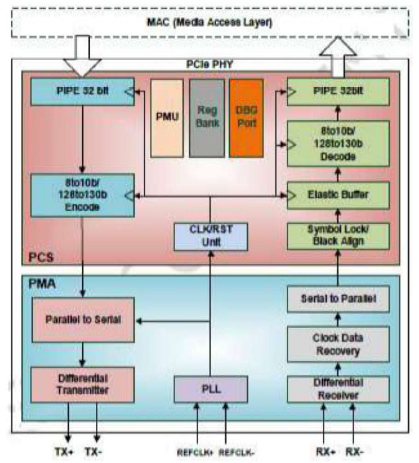
For high-bandwidth applications, the PCIe 5.0 PHY IP offers excellent performance, multi-lane capabilities, and low power design. The PCIe 5.0 IP complies with the PIPE 5.2 standard and supports the whole spectrum of PCIe 5.0 Base applications. High-speed mixed-signal circuits are included into the IP to accommodate 32Gbps PCIe 5.0 traffic.
The PCIe4.0 data rate at 16 Gbps, the PCIe 3.1 data rate at 8.0 Gbps, the PCIe 2.1 data rate at 5.0 Gbps, and the PCIe data rate at 2.5 Gbps are all backward compatible with this device. The needs for various channel conditions may be met by the PCIe 5.0 IP thanks to its support for both TX and RX equalization methods.

Compliant with PCIe 5.0 Base Specification
Compliant with PIPE 5.1
Supported data transfer rate: 2.5 GT/s, 5.0 GT/s, 8.0 GT/s, 16.0 GT/s and 32GT/s
Supported physical lane width: x4
Supported parallel interface: 16/32- bit (Gen4/5), 10/20-bit (Gen1/2/3)
Support dual-port PLL with LC tanks
Support CC/SRIS/SRNS
Support SSC for EMI reduction
DFE+CTLE for RX-EQ training
3-tap FFE for TX preset
Power-gated for lowest leakage in L1.2 low power mode (PMA)
Auto power saving for short reach
Silicon Proven in TSMC 16nm FFC
Operating Voltage: 0.8V and 1.2V
Built-in EYE-monitor and EYE checker
Deliverables
GDSII & layer map
Place-Route views (.LEF)
Liberty library (.lib)
Verilog behaviour model
Netlist & SDF timing
Layout guidelines, application notes
LVS/DRC verification reports