Compliance with the PCIe 3.0 Base Specification is standardized by the PCIe 3.0 PHY IP with PIPE 4.3 interface standard. Because the low power mode option is programmable, the PHY is also particularly useful for a variety of applications with varied power consumption needs. The inclusion of an extra PLL control, reference clock control, and built-in voltage regulation control allows for this Low power utilization. Utilizing a test bench created in Verilog HDL, NCVerilog simulation software is used to verify PCIe PHY operation.
Compliant with PCIe 3.0 Base Specification
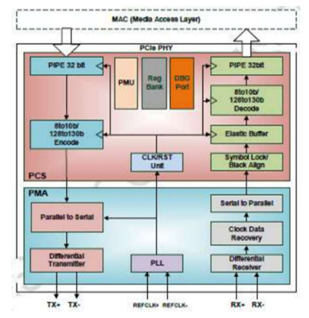
Compliant with PIPE 4.3
Supported data transfer rate: 2.5 GT/s, 5.0 GT/s and 8.0 GT/s
Supported physical lane width: x4
Supported parallel interface: 32-bit
Supported input reference clock: 100 MHz
Supported parallel interface data clock: 62.5 MHz, 125 MHz, and 250 MHz
Supporting low power operation with configurable setting in power state P1/P2/L1 PM Substates:
PLL control, reference clock control, and embedded power gating control
SMIC 40nm LP 1P7M5X1R (HVT/LVT/EHVT) process
Operating Voltage: 0.9V, 0.95V, 1.2V and 1.8V
Providing robust testability by low-cost Build-In Self- Test (BIST) via near-end analog and external loopback interface as well as far-end analog/digital loopback interface
Deliverables
Application Note / User Manual
Behavior model, and protected RTL codes
Protected Post layout netlist and
Standard Delay Format (SDF)
Synopsys library (LIB)
Frame view (LEF)
Metal GDS (GDSII)
Test patterns and Test Documentation
