The PCIe 3.0 PHY IP is designed to support increased applications with its low-power, multi-lane, high-performance design. It fully supports a wide range of PCIe 3.0 Base applications and complies with the PIPE 4.3 specification. By integrating high-speed mixed signal circuits, the IP enables PCIe 3.0 traffic at 8Gbps. It maintains backward compatibility with transfer throughputs of 5.0 Gbps for PCIe 2.0 and 2.5 Gbps for PCIe 1.0. Additionally, it caters to various channel circumstances by supporting both TX and RX equalization approaches.
Compliant with PCIe 3.0 Base Specification
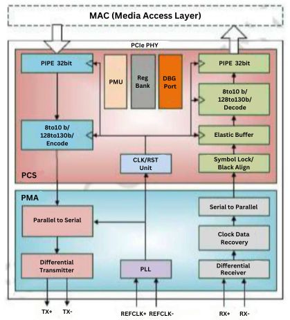
Compliant with PIPE 4.3
Supported data transfer rate: 2.5 GT/s, 5.0 GT/s and 8.0 GT/s
Supported physical lane width: x4
Supported parallel interface: 32-bit
Supported input reference clock: 100 MHz
Supported parallel interface data clock: 62.5 MHz, 125 MHz, and 250 MHz
Supporting low power operation with configurable setting in power state P1/P2/L1 PM Substates:PLL control, reference clock control, and embedded power gating control
Silicon Proven in TSMC 22ULP
Operating Voltage: 0.9V, 0.95V, 1.2V and 1.8V
Providing robust testability by low-cost Build-In Self-Test (BIST) via near-end analog and external loopback interface as well as far-end analog/digital loopback interface
Deliverables
GDSII Circuit Layout Data with Layer Mapping .
LEF Files Illustrating Placement and Routing
Library of Timing and Power Models in .lib Format
Verilog HDL Representation of Circuit Behavior
Circuit Netlist Annotated with SDF Timing Constraints
Design Guidelines and Best Practices for Layout
Reports Confirming Layout Consistency and Compliance with Design Rules
