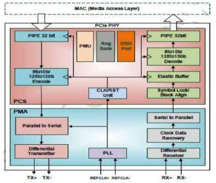
With compliance for PIPE 4.4 interface spec, Peripheral Component Interconnect Express (PCIe) Gen4 PHY IP complies with PCIe 4.0 Base Specification. Capability for additional PLL control, reference clock control, and inbuilt power gating control leads to reduced power usage. Additionally, because the previously mentioned low power mode setting is programmable, the PHY is broadly suitable for a wide range of scenarios with diverse power consumption constraints.

Compliant with PCIe 4.0 Base Specification
Compliant with PIPE 4.4
Supported data transfer rate: 2.5 GT/s, 5.0 GT/s, 8.0 GT/s and 16.0 GT/s
Supported physical lane width: x4
Supported parallel interface: 16-bit and 32-bit
Supported input reference clock: 100 MHz
Supported input crystal clock for SRIS: 25 MHz
Supported parallel interface data clock: 62.5 MHz, 125 MHz and 250 MHz and 500MHz
Supporting low power operation with configurable setting in power state P1/P2/L1 PM Substates: PLL control, reference clock control, and embedded power gating control
TSMC 28nm HPCP 1P9M4X2Y2R (HVT/LVT/EHVT/SVT) process
Operating Voltage: 0.9V, 0.95V, 1.2V and 1.8V
Wire-bond
Providing robust testability by low-cost Build-In Self-Test (BIST) via near-end analog and external loopback interface as well as far-end.
Deliverables
Application Note / User Manual
Behavior model, and protected RTL codes
Protected Post layout netlist and
Standard Delay Format (SDF)
Synopsys library (LIB)
Frame view (LEF)
Metal GDS (GDSII)
Test patterns and Test Documentation