Description
The DDR3L/ DDR4/ LPDDR4 Combo PHY IP offers low latency and supports throughput of up to 1866Mbps. The PHY IP is silicon validated in the UMC 28HPC+ process technology, complies with the most recent JEDEC requirements, is used to control DRAM devices, to access the data stored in these devices, provide SSTL135, POD12 and LVSTL interfaces for DDR3L, DDR4 and LPDDR4.
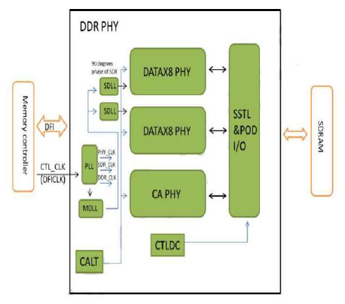
Features
-
Supported DRAM type: DDR3L/DDR4/LPDDR4
-
Maximum controller clock frequency of 400MHz resulting in maximum DRAM data rate of 1866Mbps
-
Interface: SSTL135/POD12/LVSTL
-
Data path width scales in 32-bit increment
-
Four modules for flexible configuration:CA/DQ_X16/DQ_X8/ZQ
-
Programmable output impedance (DS)
-
Programmable on-die termination (ODT)
-
Core power:0.9V, I/O power (VDDQ):1.5V/1.35V/1.2V, RX power:1.8V
-
ESD: 2KV/HBM, 200V/MM, 500V/CDM
-
Support ZQ calibration
-
Support 8 ranks
-
Support write-leveling, CBT
-
Support PHY internal VREFDQ auto decision
-
Per-bit deskew in read and write datapath
-
Silicon Proven in UMC 28HPC+ process technology
-
Supported metal scheme: 1P7M_1C
Deliverables
-
Application Note / User Manual
-
Behavior model, and protected RTL codes
-
Protected Post layout netlist and Standard Delay Format (SDF)
-
Frame view (LEF)
-
Metal GDS (GDSII)
-
Test patterns and Test Documentation
