Description
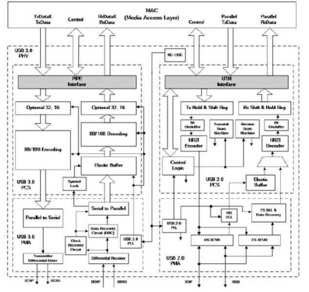
The combo PHY consist of Peripheral Component Interconnect Express (PCIe) compliant with PCIe 3.1 Base Specification with support of PIPE v4.4 interface spec, Universal Serial Bus (USB) compliant with the USB 3.2, USB 2.0 (USB High-speed and Full speed) and Serial ATA (SATA) compliant with SATA 3.2 Specification. Lower power consumption is achieved due to support of additional PLL control, reference clock control, and embedded power gating control. Also, since aforementioned low power mode setting is configurable, the PHY is widely applicable for various scenarios.
Features
-
Compliant with PCIe 3.1 Base Specification
-
Compliant with Universal Serial Bus 3.2 Specification
-
Compliant with Universal Serial Bus 2.0 Specification
-
Compliant with UTMI 1.05 Specification
-
Compliant with SATA 3.2 Specification
-
Compliant with PIPE 4.4
-
Supported data transfer rate: 2.5 GT/s, 5.0 GT/s and 8.0 GT/s (PCIe)
-
Supported data transfer rate: 5.0 GT/s and 10.0 GT/s (USB)
-
Supported data transfer rate: 1.5 GT/s, 3.0 GT/s and 6.0 GT/s (SATA)
-
High-speed data transfer rate: 480 Mbps (USB)
-
Full-speed data transfer rate: 12 Mbps (USB)
-
Supported physical lane width: x2
-
Supported parallel interface: 32-bit
-
Supported input reference clock: 100 MHz (PCIe)
-
Supported input crystal clock for SRIS: 25 MHz
-
Support crystal-less in SATA mode
-
Support low power operation with configurable setting in power state:
-
PLL control, reference clock control, and embedded power gating control
-
UMC 28nm HPCP 1P9M4X2Y2R_AL=28kA (uHVT/HVT/RVT/LVT) process
-
Operating Voltage: 0.9V, 0.95V, 1.8V and 3.3V
-
Providing robust testability by low cost Build-In-
-
Self-Test (BIST) and near/far end loopback at analog/digital interface
-
Silicon Proven in UMC 28HPC
Deliverables
-
Circuit Layout Data with Layer Allocation in GDSII
-
.LEF Files Presenting Placement and Routing Views
-
Library of Timing and Power Models in .lib Format
-
Verilog HDL Representation of Circuit Behavior
-
Circuit Netlist Annotated with SDF Timing Constraints
-
Design Guidelines and Best Practices for Layout Implementation
-
Reports Confirming Layout Consistency and Compliance with Design Rules
