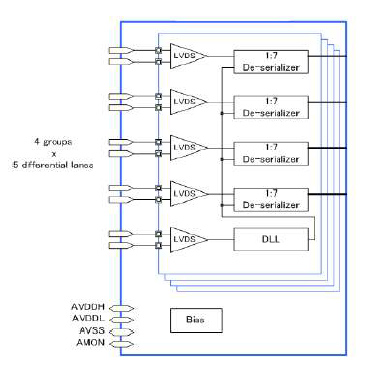
The V-by-One® HS technology aims to transmit video signals at a high data rate using internal equipment connections. The requirements to create a transmitter and receiver are laid out in the V-by-One®HS Standard. This has an available 8-lane PHY and 16-lane PHY for Tx and Rx, and it supports up to 4Gbps/lane. an LVDS Receiver physical layer IP. This IP has 20 lanes (4 x 4D1C) of LVDS receivers and can handle 1.5Gbps of data flow. There is a 25MHz to 150MHz input clock. The serializer is completely internal and doesn't need any extra parts. The circuit is modularly constructed and desensitized to handle changes. This makes process migration easier and produces a solid design.

LVDS compliant Rx
4 groups of 4-Data, 1-Clock channels
Each lane/group can be turned on/off individually
Supports from 168Mbps to 1.5Gbps data rate
Configurable analog characteristics
Bias voltage/current
DLL characteristics
Testability Internal analog nodes can be observed through a test pad DLL test mode Process
Testability At speed test by Loopback BIST
Internal analog nodes can be observed through a test pad
Supports VCO gain test, transmitter DC test, IDDQ test
Supply Voltage 1.8V/0.9V
Silicon Proven in GF 22nm FDX
Deliverables
Datasheet
Integration Guideline
GDS or Phantom GDS
Layer Map Table
CDL Netlist for LVS
LEF
Verilog Behavior Model
Liberty Timing Model
DRC/LVS/ERC results
RTL for Digital section
Test Spec Document