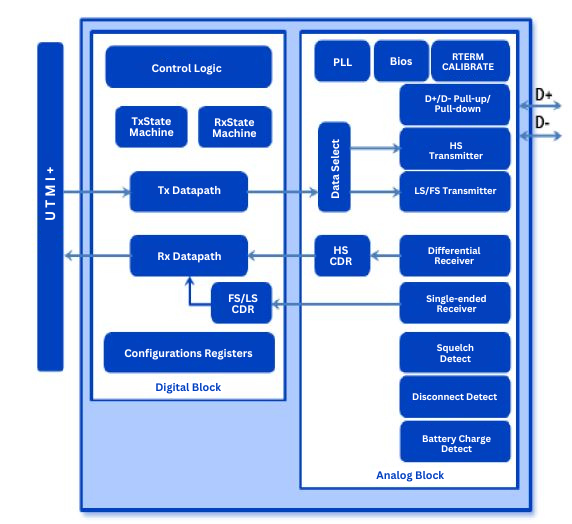
The USB 2.0 PHY IP Core is a complete solution for the physical layer (PHY) that prioritizes both high performance and low power consumption. This versatile IP core offers a High-Speed USB 2.0 transceiver compatible with host, device, and On-The-Go (OTG) function controllers. Compliant with the UTMI+ level 3 specification, the USB2.0 PHY IP also supports legacy data rates of Full-Speed (12 Mbps) and Low-Speed (1.5 Mbps). A combination of advanced mixed-signal circuits enables high-speed data transmission at 480 Mbps. Additionally, the USB2.0 PHY IP supports the latest USB Battery Charging specifications, making it ideal for mobile and consumer electronics. Despite its small size and low power consumption, the USB2.0 PHY transceiver maintains excellent performance and data throughput. For comprehensive functionality as both a host and device, the USB2.0 PHY IP provides a complete on-chip physical transceiver solution with features like Electrostatic Discharge (ESD) protection, an internal PLL for clock generation, and a resistor termination calibration circuit.

Deliverables
GDSII Physical Layout Representation with Layer Mapping Details
Representation of Placement and Routing Topography in .LEF
Liberty Format Repository housing Timing and Power Models
Functional Simulation Model represented in Verilog Syntax
SDF Timing Specifications integrated into Circuit Netlist
Guidelines for Successful Layout Construction and Execution
Verification Reports confirming Layout Schematic and Rule Conformity