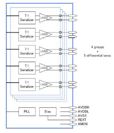
A transmitter for LVDS with a physical layer IP. This IP has 20 lanes (4 x 4D1C) of LVDS drivers and can handle 1.5Gbps of data rate. Both serial and parallel data are divided into 4 channels in LVDS mode. Each channel of the parallel data has a width of 7 bits. There is a 25MHz to 150MHz input clock. The serializer is completely internal and doesn't need any extra parts. The circuit is modularly constructed and desensitized to handle changes. This makes process migration easier and produces a solid design.

LVDS compliant Tx
4 groups of 4-Data
1-Clock channels Each lane/group can be turned on/off individually Data/Clock can be assigned to any lane within the group
Differential polarity can be flip per lane
Supports from 168Mbps to 1.5Gbps data rate
Supports reduced swing mode
X7 Multiplier PLL for serial clock generation
Configurable analog characteristics
PLL loop filter
PLL VCO gain
Differential voltage Common-mode voltage
Pre-emphasis strength
Silicon Proven in GF 65/55nm LPe.
Deliverables
Datasheet
Integration guideline
GDSII or Phantom
GDSII Layer map table
CDL netlist for LVS
LEF Verilog behavior model
Liberty timing model DRC/LVS/ERC results