The Combo PHY is a complete USB 3.0 and PCIe 2.0 PHY IP solution designed for a mobile and data consumer applications in TSMC 28nm process. It supports both USB3.0 (1 or 2 ports) and PCIe 2.0 (1 lane). It consists of Physical Coding Sublayer and Physical Media Attachment and includes all circuitry for interface operation with 8/10 encoding/decoding, driver, input buffers, PLL and impedance matching circuitry. The PHY provides standard PIPE interface with the Media Access Layer for exchanging information. Lower power consumption is achieved due to support of additional PLL control, reference clock control, and embedded power gating control. Also, since aforementioned low power mode setting is configurable, the PHY is widely applicable for various scenarios under different consideration of power consumption.
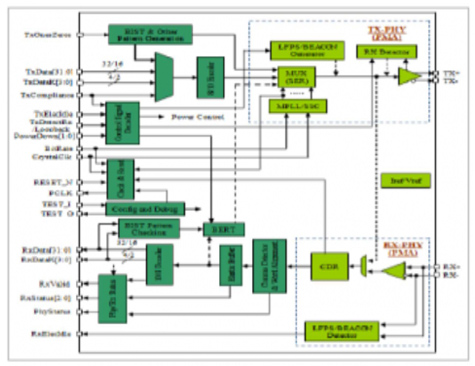
Standard PHY interface (PIPE) enables multiple IP sources for PCIe/USB3 MAC layer
Supports 2.5GT/s and 5.0GT/s serial data transmission rate
Supports 16-bit or 32-bit parallel interface
Data and clock recovery from serial stream
8b/10b encoder/decoder and error indication
Support direct disparity control for use in transmitting compliance pattern in Pole mode
Support power change and rate change at a same PCLK edge in PCIe mode
Tunable Receiver detection to detect worse case cables
Beacon transmission and reception in Pole mode
Low Frequency Periodic Signaling (LFPS) transmission and reception in USB 3.0 mode
Support SSCG function to reduce EMI effects with tunable down spread amplitude
Selectable TX margining, Tx de-emphasis and signal swing values
Internal Loopback Test Capable
Allowable analog circuit parameter adjustment and internal test control
Compliant with USB3/PCIe base specification
Silicon Proven in TSMC 28HPC+.
Deliverables
GDSII Format Including Layer Configuration
Representation of Placement and Routing in LEF Format
Standard Cell Library with Timing and Power Specifications
Behavioral Model Expressed in Verilog HDL
Netlist Including Timing Annotations in SDF Format
Layout Design Guidelines for Optimal Implementation
Validation Reports Ensuring Layout Consistency and Rule Adherence
