Description
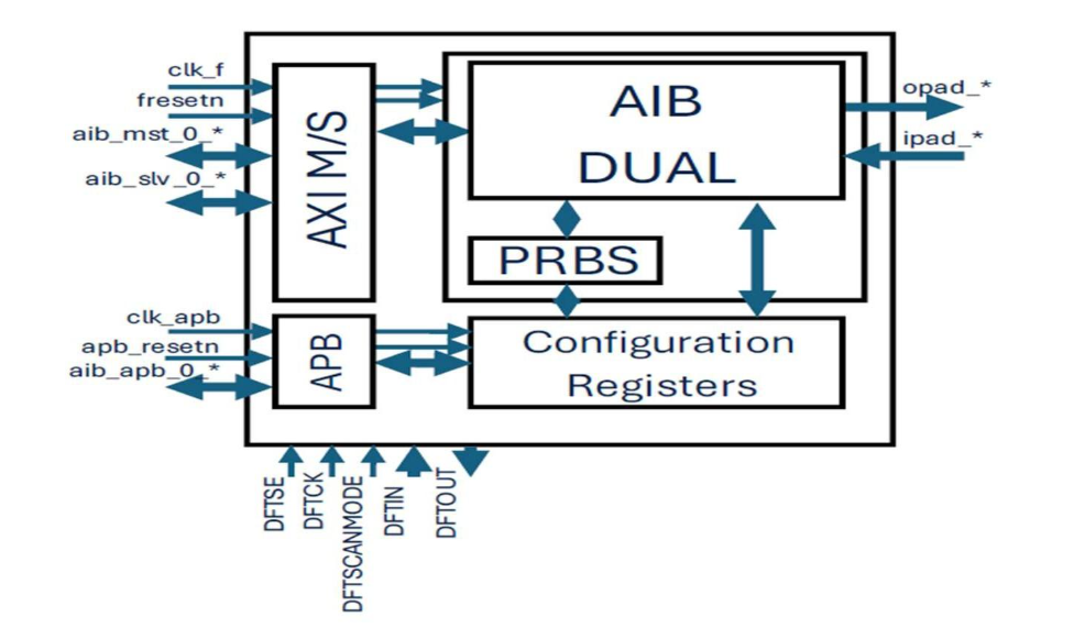
This die-to-die interconnect IP Core is defined as an AIB IP Core, which is optimized for 32-bit AXI data transfer, enabling Master-to-Slave AXI transactions in either Master or Slave configuration.
An integrated AXI protocol module converts system AXI signals to the AIB interface for transmission to a receiving AXI endpoint. This design has successfully linked an ARM NI700 and ARM NIC400 across separate dies, supporting 32-bit AXI word transfers.
The AIB interface delivers 40-bit data throughput via 20 DDR lanes. It operates at the system clock frequency for AXI and core functions, while using a lower-speed clock for APB-based configuration.
Features
-
1.6Gbps/bump 800MHz DDR
-
Throughput: 20 data lanes, 32Gbps per channel
-
Digital Supply 1.0V
-
Maximum Frequency: 800MHz
-
Latency: 12ns
-
Energy: 0.1pJ/b
-
AXI Bridge (Master, Slave)
-
APB configuration
-
PRBS for Self-test
-
DCC + Digital DLL compensation
-
Input clocks: up to 800MHz from AXI, up to 100MHz from APB
-
Digital 1GHz full-swing IO Driver
-
Digital weak pull-up/pull-down
-
Error Correction Code
-
Latency reduction logic
-
Process: ST 28nm FDSOI 0.9V to 1.10V
-
Metal Scheme: 10ML (38 mask)
-
VT Options: LVT
Deliverables
-
Extensive Product Documentation
-
Verilog Model (A) for Simulation Purposes
-
Liberty Database (.db/.lib) for Synthesis, Timing Analysis, and Equivalence Verification
-
Design Verification with CTL/CTLDB Techniques
-
ATPG Utilizing SPF (STIL Procedure File)
-
Layout Exchange Format (LEF) for Automated Place and Route (APR)
-
Circuit Description Language (CDL) for Layout Versus Schematic (LVS) Alignment